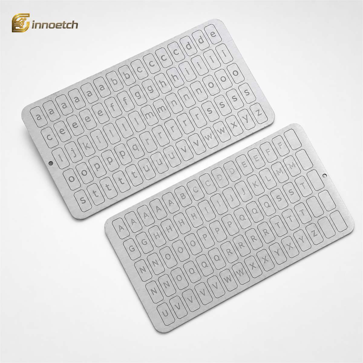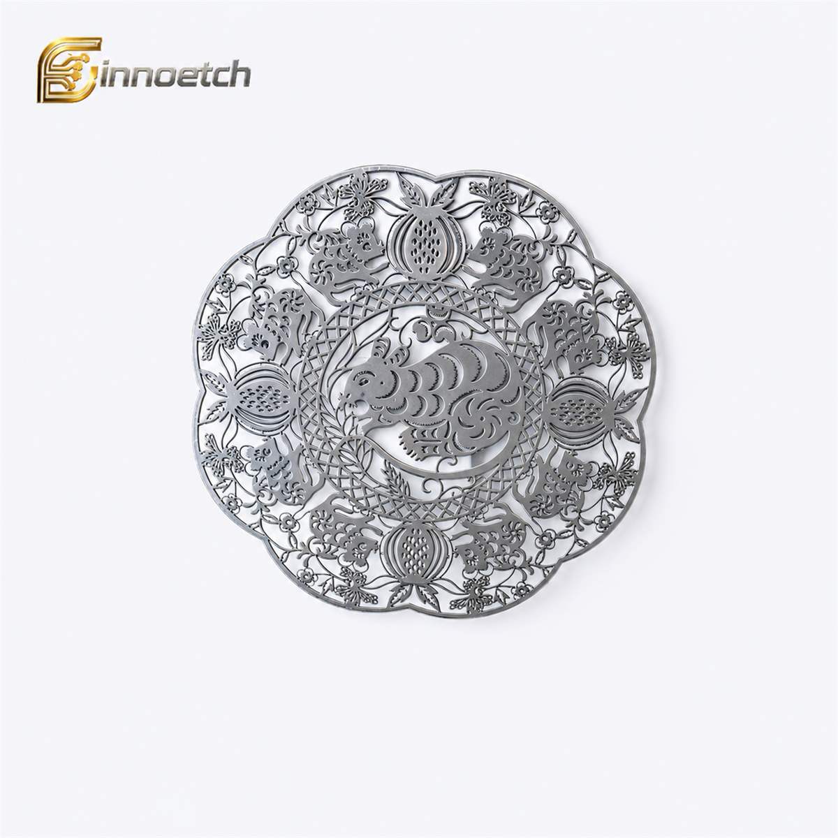
Outlines the photo etching workflow from CAD review and tooling to sample validation, process control, and mass production.
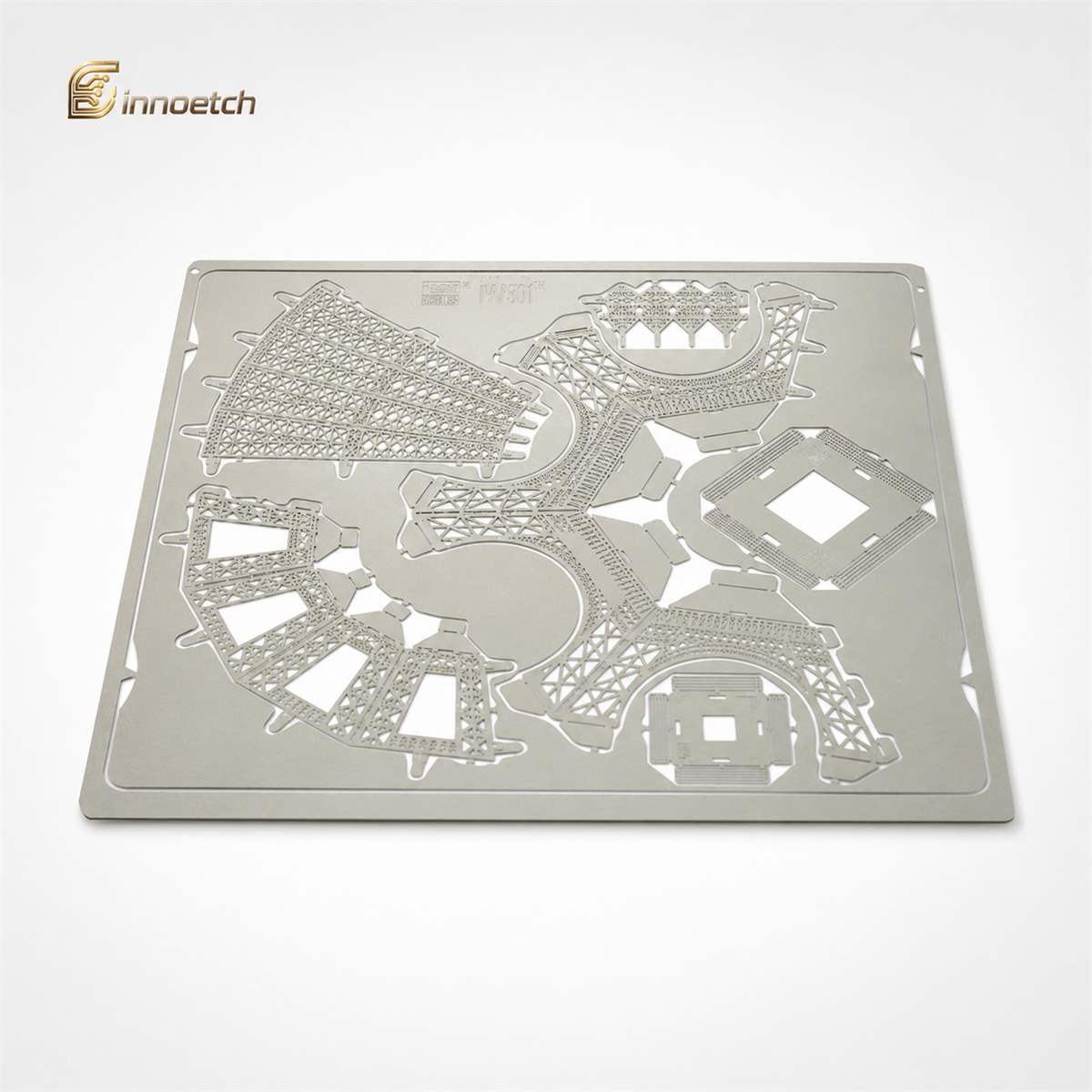
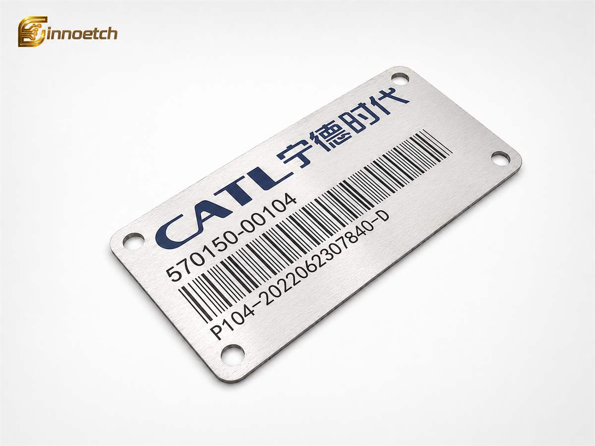
Photo etching, also known as photochemical etching, chemical etching, or precision metal etching, is a manufacturing process used to produce thin, complex, burr-free metal parts. It is widely used for precision metal mesh, shims, electronic components, shielding parts, filters, speaker grilles, springs, mechanical parts, structural parts, ornaments, and nameplates.
For engineers, one of the biggest advantages of photo etching is that the same process can support both prototype development and mass production. A design can be tested, adjusted, validated, and scaled without the high tooling cost usually associated with hard stamping dies.
Below is a step-by-step FAQ explaining how the photo etching process works from prototype to mass production.
The process usually begins with a technical review of the customer’s CAD drawing, material requirement, application, tolerance, quantity, and expected production volume.
At this stage, engineers should provide:
A complete drawing package helps the etching manufacturer evaluate feasibility, cost, lead time, and production risk more accurately.
DFM, or design for manufacturing, is essential before photo etching prototypes are made. A part may look correct in CAD but still have features that are too small, too fragile, or difficult to control in production.
During DFM review, the manufacturer checks:
Early DFM review helps prevent sampling delays, rework, and unnecessary cost before tooling begins.
Material selection depends on the part’s function, strength, corrosion resistance, conductivity, elasticity, appearance, and working environment.
Common materials include stainless steel, copper, brass, nickel, aluminum, molybdenum, and specialty alloys. Stainless steel is often used for corrosion resistance and mechanical strength. Copper and copper alloys are useful for electrical conductivity. Nickel alloys may be used for battery components, springs, and high-performance electronic applications.
Material thickness also affects minimum feature size, tolerance, edge profile, and production yield, so it should be confirmed before prototype tooling.
Photo tooling is the artwork used to transfer the part geometry onto the metal sheet. It is usually created from the customer’s CAD data.
Unlike hard stamping dies, photo tooling is more flexible and cost-effective for prototypes and design changes. If the engineer needs to adjust hole size, mesh density, slot width, or outer profile, the artwork can often be updated more easily than a mechanical die.
This is one reason photo etching is well suited for prototype development and product iteration.
Before etching, the metal sheet must be cleaned to remove oil, dust, oxidation, and surface contamination. A clean surface helps the photoresist adhere properly and improves pattern accuracy.
After cleaning, a photosensitive resist is applied to the metal sheet. This resist protects the areas that should remain after etching.
Good surface preparation is important for consistent feature definition, stable tolerances, and repeatable quality.
During exposure, the prepared metal sheet is aligned with the photo tooling and exposed to controlled light. The light transfers the pattern onto the photoresist.
After exposure, the sheet is developed. The development step removes selected resist areas and reveals the metal that will be chemically etched away.
Accurate exposure and development are important for fine holes, dense mesh patterns, narrow slots, half-etched features, and precision outlines.
In the etching stage, the developed metal sheet passes through a controlled chemical etching process. The etchant removes exposed metal areas while the protected areas remain.
This process can create:
Because the process does not use mechanical cutting force, it can produce burr-free parts with low stress and minimal distortion.
After the required metal has been removed, the remaining photoresist is stripped away. The parts are then cleaned and prepared for inspection or secondary processing.
Depending on the application, post-etching steps may include:
For functional parts, post-processing should be specified before production so the manufacturer can include it in the process plan.
Prototype inspection confirms whether the etched parts meet drawing requirements and functional expectations.
Inspection may include:
Prototype samples are also tested by the customer for assembly, airflow, filtration, electrical performance, shielding, spring behavior, or cosmetic appearance.
If the prototype does not fully meet performance or assembly requirements, the design can be revised. This is one of the major advantages of photo etching.
Common prototype adjustments include:
Because photo etching uses digital artwork and photo tooling, design changes are usually easier and less expensive than modifying hard stamping tools.
Pilot production is the stage between prototype approval and full mass production. It helps confirm whether the approved design can be produced consistently at a larger scale.
During pilot production, the manufacturer verifies:
Pilot production reduces the risk of moving too quickly from prototype samples to high-volume manufacturing.
Once the prototype and pilot run are approved, the process can move into mass production. At this stage, the focus shifts from design validation to repeatability, efficiency, quality control, and delivery stability.
Mass production control usually includes:
INNOETCH supports custom precision metal etching from prototype development to mass production, with engineering support and quality management for precision etched components.
Quality control is critical in mass production because small dimensional changes can affect assembly, airflow, conductivity, filtration, shielding, or mechanical performance.
Common quality controls include:
For industries such as electronics, semiconductor components, filtration, mechanical systems, and precision assemblies, consistent quality is just as important as the first successful prototype.
Photo etching is efficient because it combines design flexibility with repeatable manufacturing. Engineers can start with prototypes, make design changes, validate performance, and then scale the same process for production.
Key advantages include:
This makes photo etching especially useful for custom metal parts that require precision, flexibility, and consistent quality.
The prototype-to-mass-production workflow is commonly used for:
These parts often require fine detail, thin materials, burr-free edges, and repeatable dimensional accuracy.
The photo etching process from prototype to mass production begins with CAD review and DFM analysis, then moves through material selection, photo tooling, resist coating, exposure, development, chemical etching, cleaning, inspection, prototype validation, pilot production, and controlled batch manufacturing.
For engineers developing custom thin metal parts, photo etching offers a practical path from early design testing to reliable mass production. Working with an experienced precision metal etching manufacturer such as INNOETCH can help improve manufacturability, reduce development risk, shorten iteration cycles, and ensure stable quality for custom etched metal components.
How Does the Photo Etching Process Work from Prototype to Mass Production? is widely used in precision metal etching applications where clean edges, tight tolerances, complex patterns and stable performance are required. Typical industries include electronics, semiconductors, sensors, fuel cells, acoustic components, EMI shielding, thermal management and precision mechanical parts.
How Does the Photo Etching Process Work from Prototype to Mass Production? is a precision metal component manufactured by photochemical etching for applications requiring accurate dimensions, smooth edges and reliable performance.
Common materials include stainless steel, copper, brass, nickel silver, titanium, aluminum and other thin metal sheets depending on the application requirements.
INNOETCH can process thin metal materials from approximately 0.02 mm to 1.5 mm, depending on material type, part structure and tolerance requirements.
For many precision etched parts, tolerances can reach ±0.01 mm to ±0.05 mm, depending on material thickness, design complexity and production volume.
Chemical etching does not require expensive hard tooling and can produce fine patterns, complex shapes and burr-free edges without mechanical deformation.
Yes. INNOETCH supports custom drawings, materials, thicknesses, hole patterns, surface finishes, dimensions and prototype-to-mass-production requirements.
2D drawings, DXF files, DWG files, STEP files, material requirements, thickness, tolerance, quantity and application details are recommended for accurate quotation.
You can send your drawings and technical requirements to INNOETCH. Our engineering team will review the design and provide a quotation.