Explains IC lead frames, their role in semiconductor packaging, and why etched metal patterns support fine conductive structures.
An IC lead frame is the internal metal structure of a semiconductor package. It holds the chip in place and connects the chip to the outside circuit through metal leads. It also provides mechanical support and a thermal path for heat dissipation.
IC lead frames are commonly made from copper alloy, iron-nickel alloy, nickel alloy, stainless steel, or other conductive metal materials. They are used in integrated circuits, sensors, power devices, LED packages, automotive electronics, and consumer electronics.
The main function of an IC lead frame is to create a reliable bridge between the semiconductor chip and the external circuit board.
A typical IC lead frame performs four key roles:
Without a stable lead frame, wire bonding, soldering, encapsulation, and final device performance may be affected.
An IC lead frame usually includes a die pad, leads, tie bars, connecting bridges, positioning holes, and outer frame structures.
The die pad is the central area where the semiconductor chip is mounted. The leads connect the chip to external circuits. Tie bars and connecting bridges hold the structure together during manufacturing. Positioning holes help support accurate alignment during assembly and packaging.
Depending on the package type, the lead frame may also include half-etched areas, downset structures, heat dissipation pads, or customized array layouts.
IC lead frames are commonly made from conductive and dimensionally stable metal materials.
Copper alloy is widely used because it offers excellent electrical conductivity, thermal conductivity, and processability. Iron-nickel alloy is used when dimensional stability and thermal expansion matching are important. Nickel alloy, stainless steel, and other specialty metals may also be selected depending on package design, strength, corrosion resistance, and plating requirements.
Surface finishes may include silver plating, nickel plating, tin plating, palladium, gold, or other coatings depending on bonding and soldering requirements.
IC lead frames can be manufactured by stamping, chemical etching, or a combination of processes. For high-volume simple designs, stamping can be efficient. For fine-pitch, complex, thin, or customized structures, chemical etching offers important advantages.
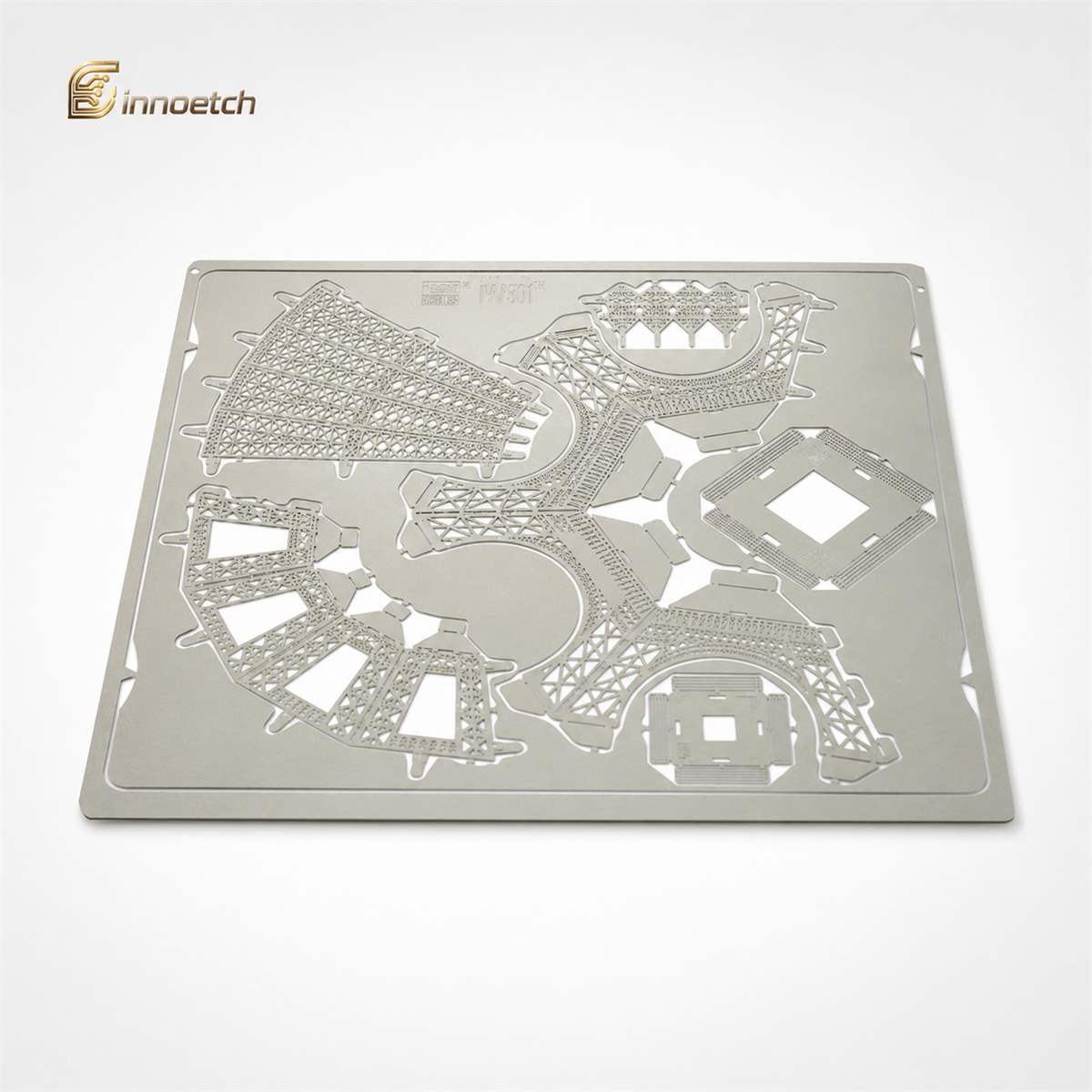
In precision metal etching, the lead frame pattern is transferred onto a metal sheet using photoresist. Exposed metal areas are then removed by a controlled chemical solution. This process can create fine leads, small gaps, positioning holes, half-etched features, and array structures with clean edges and stable dimensions.
A typical etched IC lead frame workflow includes:
Chemical etching is ideal for custom IC lead frames because it can produce fine details without mechanical stress. Unlike stamping, it does not require expensive hard tooling for every design change. This makes it suitable for prototypes, small batches, engineering validation, and complex semiconductor packaging components.
Chemical etching also helps reduce burrs, deformation, and stress-related flatness issues. This is important because unstable lead dimensions, poor flatness, or rough edges can affect wire bonding, soldering, mounting, and encapsulation.
For high-density leads, thin materials, and complex array designs, etched IC lead frames provide excellent design flexibility and stable batch quality.
IC lead frames are used in many semiconductor and electronics applications, including:
Integrated circuit packages
Sensor packages
Power semiconductor devices
LED packages
Electronic connectors
Automotive electronics
Industrial electronics
Consumer electronics
Miniature electronic assemblies
Custom semiconductor package components
They are especially important when a package needs stable electrical connection, mechanical support, thermal performance, and reliable mass production quality.
Q1: What is an IC lead frame used for?
An IC lead frame is used to support the chip, connect it electrically to external circuits, help dissipate heat, and maintain structural stability inside a semiconductor package.
Q2: What materials are used for IC lead frames?
Common materials include copper alloy, iron-nickel alloy, nickel alloy, stainless steel, and other conductive metal materials.
Q3: Why is copper alloy commonly used for lead frames?
Copper alloy is widely used because it provides high electrical conductivity, good thermal conductivity, and strong manufacturability for semiconductor packaging.
Q4: Can IC lead frames be made by chemical etching?
Yes. Chemical etching is suitable for fine-pitch, thin, complex, and customized IC lead frames because it produces accurate features with clean edges and low mechanical stress.
Q5: What is the difference between stamped and etched lead frames?
Stamped lead frames are made with mechanical dies and are efficient for stable high-volume designs. Etched lead frames are made by chemical removal and are better for complex geometries, prototypes, fine features, and flexible design changes.
Q6: Why is lead frame quality important?
Lead frame quality affects wire bonding, soldering, heat dissipation, package alignment, electrical performance, and semiconductor device reliability.
An IC lead frame is a critical metal component in semiconductor packaging. It supports the chip, provides electrical pathways, helps manage heat, and ensures stable connection between the semiconductor device and the external circuit.
For custom IC lead frames, sensor lead frames, power device lead frames, LED package frames, and other semiconductor packaging metal components, precision metal etching offers a flexible and reliable manufacturing method from prototype development to mass production.
What Is an IC Lead Frame? is widely used in precision metal etching applications where clean edges, tight tolerances, complex patterns and stable performance are required. Typical industries include electronics, semiconductors, sensors, fuel cells, acoustic components, EMI shielding, thermal management and precision mechanical parts.
What Is an IC Lead Frame? is a precision metal component manufactured by photochemical etching for applications requiring accurate dimensions, smooth edges and reliable performance.
Common materials include stainless steel, copper, brass, nickel silver, titanium, aluminum and other thin metal sheets depending on the application requirements.
INNOETCH can process thin metal materials from approximately 0.02 mm to 1.5 mm, depending on material type, part structure and tolerance requirements.
For many precision etched parts, tolerances can reach ±0.01 mm to ±0.05 mm, depending on material thickness, design complexity and production volume.
Chemical etching does not require expensive hard tooling and can produce fine patterns, complex shapes and burr-free edges without mechanical deformation.
Yes. INNOETCH supports custom drawings, materials, thicknesses, hole patterns, surface finishes, dimensions and prototype-to-mass-production requirements.
2D drawings, DXF files, DWG files, STEP files, material requirements, thickness, tolerance, quantity and application details are recommended for accurate quotation.
You can send your drawings and technical requirements to INNOETCH. Our engineering team will review the design and provide a quotation.